- 您现在的位置:买卖IC网 > Sheet目录354 > RDK-242 (Power Integrations)KIT REF DESIGN VG TOPSWITCH-JX
�� �
�
�TOP264-271�
�mode.� As� can� be� seen� in� Figures� 27� and� 28,� the� benefits� of� jitter�
�increase� with� the� order� of� the� switching� harmonic� due� to� an�
�increase� in� frequency� deviation.� The� FREQUENCY� pin� offers� a�
�switching� frequency� option� of� 132� kHz� or� 66� kHz.� In� applications�
�that� require� heavy� snubber� on� the� drain� node� for� reducing� high�
�frequency� radiated� noise� (for� example,� video� noise� sensitive�
�applications� such� as� VCRs,� DVDs,� monitors,� TVs,� etc.),� operating�
�at� 66� kHz� will� reduce� snubber� loss,� resulting� in� better� efficiency.�
�Also,� in� applications� where� transformer� size� is� not� a� concern,� use�
�of� the� 66� kHz� option� will� provide� lower� EMI� and� higher� efficiency.�
�Note� that� the� second� harmonic� of� 66� kHz� is� still� below� 150� kHz,�
�above� which� the� conducted� EMI� specifications� get� much� tighter.�
�For� 10� W� or� below,� it� is� possible� to� use� a� simple� inductor� in� place�
�of� a� more� costly� AC� input� common� mode� choke� to� meet�
�worldwide� conducted� EMI� limits.�
�Transformer� Design�
�It� is� recommended� that� the� transformer� be� designed� for�
�maximum� operating� flux� density� of� 3000� Gauss� and� a� peak� flux�
�density� of� 4200� Gauss� at� maximum� current� limit.� The� turns� ratio�
�should� be� chosen� for� a� reflected� voltage� (V� OR� )� no� greater� than�
�135� V� when� using� a� Zener� clamp� or� 150� V� (max)� when� using� an�
�RCD� clamp� with� current� limit� reduction� with� line� voltage� (overload�
�protection).� For� designs� where� operating� current� is� significantly�
�lower� than� the� default� current� limit,� it� is� recommended� to� use� an�
�externally� set� current� limit� close� to� the� operating� peak� current� to�
�reduce� peak� flux� density� and� peak� power� (see� Figure� 18).�
�Standby� Consumption�
�Frequency� reduction� can� significantly� reduce� power� loss� at� light�
�or� no-load,� especially� when� a� Zener� clamp� is� used.� For� very�
�low� secondary� power� consumption,� use� a� TL431� regulator� for�
�closely� between� their� respective� pin� and� SOURCE.� Once� again,�
�the� SOURCE� connection� trace� of� these� components� should� not�
�be� shared� by� the� main� MOSFET� switching� currents.� It� is� very�
�critical� that� SOURCE� pin� switching� currents� are� returned� to� the�
�input� capacitor� negative� terminal� through� a� separate� trace� that� is�
�not� shared� by� the� components� connected� to� CONTROL,�
�VOLTAGE� MONITOR� or� EXTERNAL� CURRENT� LIMIT� pins.� This�
�is� because� the� SOURCE� pin� is� also� the� controller� ground�
�reference� pin.� Any� traces� to� the� V,� X� or� C� pins� should� be� kept�
�as� short� as� possible� and� away� from� the� DRAIN� trace� to� prevent�
�noise� coupling.� VOLTAGE� MONITOR� resistors� (R� LS� in� Figures�
�14,� 15,� 19,� 22,� 23,� 26,� 30)� and� primary� side� OVP� circuit�
�components� V� ZOV� /R� OV� in� Figures� (29,� 30)� should� be� located�
�close� to� the� V� pin� to� minimize� the� trace� length� on� the� V� pin� side.�
�Resistors� connected� to� the� V� or� X� pin� should� be� connected� as�
�close� to� the� bulk� cap� positive� terminal� as� possible� while� routing�
�these� connections� away� from� the� power� switching� circuitry.� In�
�addition� to� the� 47� m� F� CONTROL� pin� capacitor,� a� high� frequency�
�bypass� capacitor� (C� BP� )� in� parallel� should� be� used� for� better� noise�
�immunity.� The� feedback� optocoupler� output� should� also� be�
�80�
�70�
�60�
�50�
�40�
�30�
�20�
�-10�
�feedback� control.� A� typical� TOP264-271� circuit� automatically�
�enters� MCM� mode� at� no-load� and� the� low� frequency� mode� at�
�light� load,� which� results� in� extremely� low� losses� under� no-load�
�0�
�-10�
�EN55022B� (QP)�
�EN55022B� (AV)�
�or� standby� conditions.�
�-20�
�0.15�
�1�
�10�
�30�
�High� Power� Designs�
�The� TOP264-271� family� contains� parts� that� can� deliver� up� to�
�162� W.� High� power� designs� need� special� considerations.�
�Frequency� (MHz)�
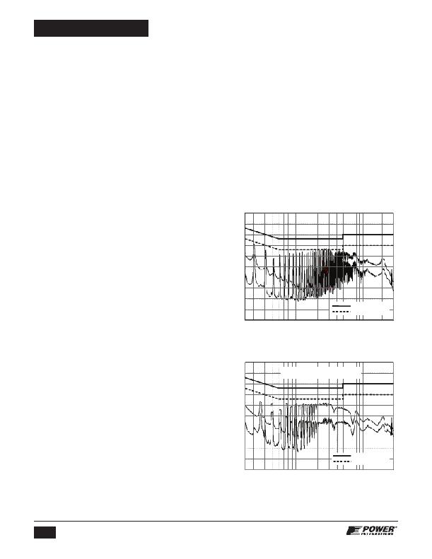
�Figure� 27.� Fixed� Frequency� Operation� Without� Jitter.�
�Guidance� for� high� power� designs� can� be� found� in� the� Design�
�Guide� for� TOP264-271� (AN-47).�
�TOP264-271� Layout� Considerations�
�The� TOP264-271� has� multiple� pins� and� may� operate� at� high�
�power� levels.� The� following� guidelines� should� be� carefully�
�followed.�
�Primary� Side� Connections�
�Use� a� single� point� (Kelvin)� connection� at� the� negative� terminal� of�
�the� input� filter� capacitor� for� the� SOURCE� pin� and� bias� winding�
�80�
�70�
�60�
�50�
�40�
�30�
�20�
�-10�
�TOPSwitch-JX (with jitter)�
�return.� This� improves� surge� capabilities� by� returning� surge�
�currents� from� the� bias� winding� directly� to� the� input� filter� capacitor.�
�The� CONTROL� pin� bypass� capacitor� should� be� located� as�
�close� as� possible� to� the� SOURCE� and� CONTROL� pins,� and� its�
�SOURCE� connection� trace� should� not� be� shared� by� the� main�
�0�
�-10�
�-20�
�0.15�
�1�
�EN55022B� (QP)�
�EN55022B� (AV)�
�10�
�30�
�MOSFET� switching� currents.� All� SOURCE� pin� referenced�
�components� connected� to� the� VOLTAGE� MONITOR� (V� pin)� or�
�EXTERNAL� CURRENT� LIMIT� (X� pin)� pins� should� also� be� located�
�20�
�Rev.� E� 08/12�
�Frequency� (MHz)�
�Figure� 28.� TOPSwitch-JX� Full� Range� EMI� Scan� (132� kHz� With� Jitter)� With�
�Identical� Circuitry� and� Conditions.�
�www.powerint.com�
�发布紧急采购,3分钟左右您将得到回复。
相关PDF资料
RJCSE538001
CONN MOD JACK 8P8C SMT R/A
RJE031882420
CONN MOD JACK 8P/8C S-FLANGES
RJE051660310
CONN MOD JACK 6P/6C UNSHIELDED
RJE051880110
CONN MOD JACK 8/8 R/A UNSHIELDED
RJE051881310
CONN MOD JACK 8P/8C SHIELDED
RJE051AA1310
CONN MOD JACK 10P/10C SHIELDED
RJE061881120
CONN MOD JACK 8P/8C VERT-MOUNT
RJE081880110
CONN MOD JACK 8P/8C UNSHIELDED
相关代理商/技术参数
RDK-248
功能描述:LED 照明开发工具 UNIVERSAL PFC 180W HiperPFS KIT
RoHS:否 制造商:Fairchild Semiconductor 产品:Evaluation Kits 用于:FL7732 核心: 电源电压:120V 系列: 封装:
RDK-249
功能描述:线性和开关式电源 HiperTFS Ref Des Kit 14.W Stby, 300W PS RoHS:否 制造商:TDK-Lambda 产品:Switching Supplies 开放式框架/封闭式:Enclosed 输出功率额定值:800 W 输入电压:85 VAC to 265 VAC 输出端数量:1 输出电压(通道 1):20 V 输出电流(通道 1):40 A 商用/医用: 输出电压(通道 2): 输出电流(通道 2): 安装风格:Rack 长度: 宽度: 高度:
RDK-251
功能描述:LED 照明开发工具 LinkSwitch-PL Ref Des Kit, 5W Dim RoHS:否 制造商:Fairchild Semiconductor 产品:Evaluation Kits 用于:FL7732 核心: 电源电压:120V 系列: 封装:
RDK-252
功能描述:电源管理IC开发工具 CAPZero Ref Des Kit CAPZero
RoHS:否 制造商:Maxim Integrated 产品:Evaluation Kits 类型:Battery Management 工具用于评估:MAX17710GB 输入电压: 输出电压:1.8 V
RDK-257
功能描述:LED 照明开发工具 RefDesign 12W90-265V LinkSwitch-PH
RoHS:否 制造商:Fairchild Semiconductor 产品:Evaluation Kits 用于:FL7732 核心: 电源电压:120V 系列: 封装:
RDK-268
功能描述:LED 照明开发工具 RefDesign 1.1W 85-265V LinkSw-PL
RoHS:否 制造商:Fairchild Semiconductor 产品:Evaluation Kits 用于:FL7732 核心: 电源电压:120V 系列: 封装:
RDK-271
功能描述:LED 照明开发工具 LED PFC DRIVER KIT 4.5W E17 LAMP
RoHS:否 制造商:Fairchild Semiconductor 产品:Evaluation Kits 用于:FL7732 核心: 电源电压:120V 系列: 封装:
RDK-290
功能描述:LED 照明开发工具 REF DESIGN RDR-290 USING LNK420EG
RoHS:否 制造商:Fairchild Semiconductor 产品:Evaluation Kits 用于:FL7732 核心: 电源电压:120V 系列: 封装: